STK672-040
SANYO Electric Co., Ltd. Semiconductor Business Headquarters
TOKYO OFFICE Tokyo Bldg., 1-10, 1 Chome, Ueno, Taito-ku, TOKYO, 110 JAPAN
10997HA(ID) / 110896HA(ID) No. 5227--1/11
Ordering number: EN 5227A
Thick Film Hybrid IC
Microstep Operation-Supported
4-Phase Stepping Motor Driver (I
O
= 1.5A)
Overview
The STK672-040 is a unipolar constant-current chopper-
type externally-excited 4-phase stepping motor driver
hybrid IC which uses MOSFET power devices. It has a
microstep operation-supported 4-phase distributed con-
troller built-in to realize a high torque, low vibration, low
noise stepping motor driver using a simple control circuit.
Applications
∑ Printer, copier, and X-Y plotter stepping motor drivers
Features
∑ Microstep sine-wave driver operation using only an
external clock input (0.33
current detection resistor
built-in)
∑ Microstep drive using only an external reference voltage
setting resistor
∑ 2, 1-2, W1-2, 2W1-2, 4W1-2 phase excitation selectable
using external pins
∑ Selectable vector locus (perfect circle mode, inside 1
mode, outside 2 modes) to match motor characteristics
in microstep drive state
∑ Phase hold function during excitation switching
∑ Schmitt trigger inputs with built-in pull-up resistor
(20k
)
∑ Monitor output pin enabling real-time confirmation of
IC excitation
∑ The CLK and RETURN inputs provide an internal
noise elimination circuit as well as CMOS Schmitt cir-
cuit to prevent malfunction due to impulse noise.
∑ 4-phase distribution switch timing selected externally to
either CLK rising-edge only detection mode or both ris-
ing-edge and falling-edge detection mode
∑ ENABLE pin for excitation current cutoff, thereby
reducing system current drain when driver is stopped
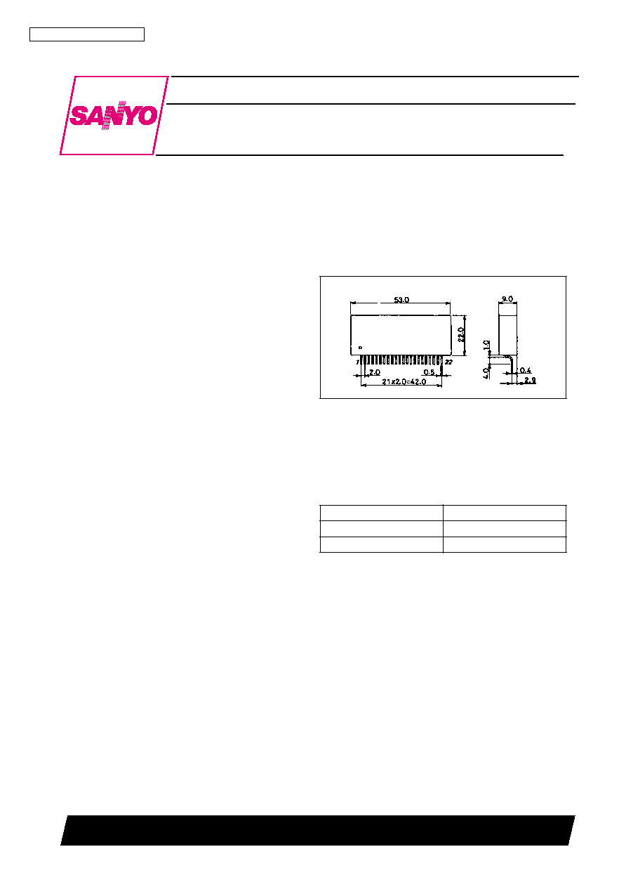
Package Dimensions
unit: mm
4161
Series Organization
The following devices form a series with differing output
capacity.
[STK672-040]
Type No.
Output current (A)
STK672-040
1.5
STK672-050
3.0
STK672-040
No. 5227--2/11
Specifications
Maximum Ratings
at Ta = 25
∞
C
Allowable Operating Ranges
at Ta = 25
∞
C
Electrical Characteristics
at Tc = 25
∞
C, V
CC
1 = 24V, V
CC
2 = 5V
Parameter
Symbol
Conditions
Ratings
Unit
Maximum supply voltage 1
V
CC
1 max
No signal
52
V
Maximum supply voltage 2
V
CC
2 max
No signal
-
0.3 to +7.0
V
Input voltage
V
IN
max
Logic input block
-
0.3 to +7.0
V
Phase output current
I
OH
max
One 0.5s pulse, V
CC
1 applied,
Load/phase: R = 5
, L = 10mH
2.2
A
Repetitive avalanche handling capability
Ear max
38
mJ
Maximum output dissipation
Pd max
c≠a = 0
12
W
Operating substrate temperature
Tc max
105
∞
C
Junction temperature
Tj max
150
∞
C
Storage temperature
Tstg
-
40 to +125
∞
C
Parameter
Symbol
Conditions
Ratings
Unit
Supply voltage 1
V
CC
1
With signal
10 to 45
V
Supply voltage 2
V
CC
2
With signal
5.0
±
5%
V
Input voltage
V
IH
0 to V
CC
2
V
Phase driver withstand voltage
V
DSS
Tr1, 2, 3, 4 (A, A, B, B outputs)
100 (min)
V
Phase current
I
OH
max
50% duty
1.5 (max)
A
Parameter
Symbol
Conditions
min
typ
max
Unit
Control supply current
I
CC
Pin 7 input, ENABLE = low
≠
4.5
15
mA
Output saturation voltage
Vsat
R
L
= 15
(I = 1.5A)
≠
1.4
1.9
V
Average output current
Io ave
Vref = 1V,
Load/phase: R = 3.5
, L = 3.8mH
0.465
0.517
0.569
A
FET diode forward voltage
Vdf
If = 1.0A
≠
1.2
1.8
V
[Control inputs]
Input voltage
V
IH
Excluding Vref pin
4.0
≠
≠
V
V
IL
Excluding Vref pin
≠
≠
1.0
V
Input current
I
IH
Excluding Vref pin
0
1
10
µ
A
I
IL
Excluding Vref pin
125
250
510
µ
A
[Vref input]
Input voltage
V
I
Pin 8
0
≠
2.5
V
Input current
I
I
Pin 8
≠
1
≠
µ
A
[Control outputs]
Output voltage
V
OH
I =
-
3mA (MoI, Mo1, Mo2 pins)
2.4
≠
≠
V
V
OL
I = +3mA (MoI, Mo1, Mo2 pins)
≠
≠
0.4
V
PWM frequency
fc
37
47
57
kHz
[Current division ratio (A/B)]
2W1-2, W1-2, 1-2
Vref
= 1/8
100
%
2W1-2, W1-2
Vref
= 2/8
92
%
2W1-2
Vref
= 3/8
83
%
2W1-2, W1-2, 1-2
Vref
= 4/8
71
%
STK672-040
No. 5227--3/11
Note: All tests are made using a constant-voltage supply.
The current division ratio shows the design value.
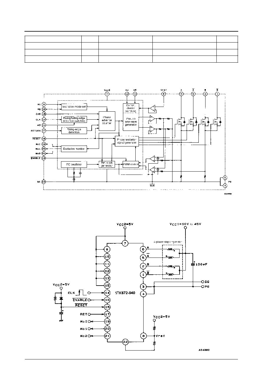
Equivalent Block Diagram
Sample Application Circuit
2W1-2 phase excitation (microstep operation)
2W1-2
Vref
= 5/8
55
%
2W1-2, W1-2
Vref
= 6/8
40
%
2W1-2
Vref
= 7/8
20
%
2
Vref
100
%
STK672-040
No. 5227--4/11
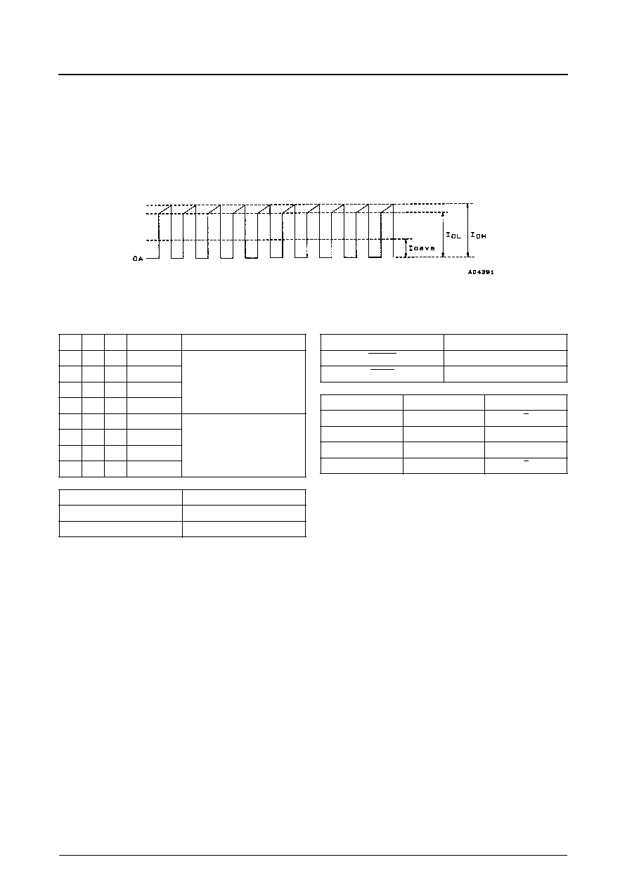
Motor Current Calculation
The motor current I
OH
is determined by the reference volt-
age on pin 8 (Vref). The relationship between I
OH
and
Vref is given by the following equation.
where Rs is the built-in current detection resistance
(0.33
±
3%).
The motor current ranges from the current due to the fre-
quency duty set by the oscillator (0.05 to 0.1A) to the
allowable operating range maximum of I
OH
= 1.5A.
Function Tables
I
OH
1
3
---
Vref Rs
/
◊
=
Motor current waveform
M1
M2
M3
Excitation
Phase switching CLK edge timing
0
0
0
Phase 1-2
Rising and falling edge
0
1
0
Phase 2W1-2
1
0
0
Phase W1-2
1
1
0
Phase 4W1-2
0
0
1
Phase 2
Rising edge only
0
1
1
Phase W1-2
1
0
1
Phase 1-2
1
1
1
Phase 2W1-2
CWB
Direction
0
Forward
1
Reverse
Input
Active level
ENABLE
Low
RESET
Low
Mo1
Mo2
Output
0
0
A
0
1
B
1
0
A
1
1
B
STK672-040
No. 5227--5/11
Design material
1. Explanation of input pins
2. Functions and timing of input signals
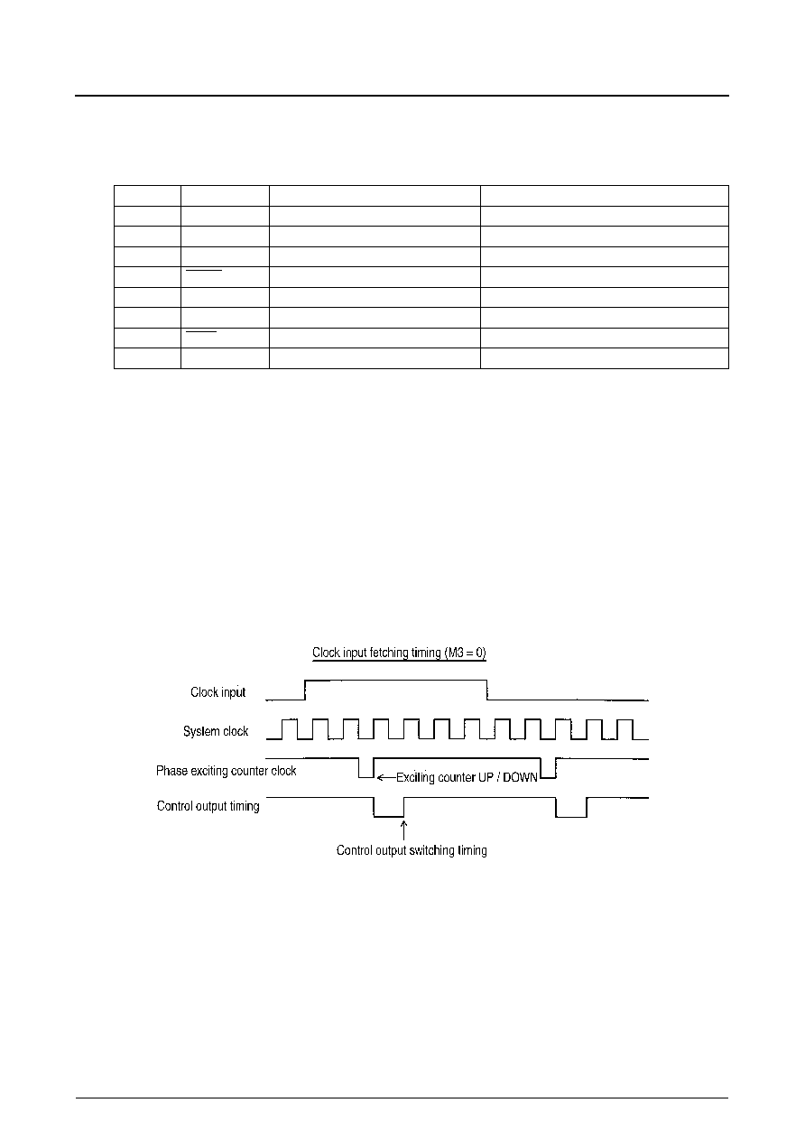
2-1. CLK (Phase switching clock)
1. Input frequency range
s
DC to 50 kHz
2. Minimum pulse width
s
10
µ
s
3. Duty
s
40 to 60%
4. Pin format
s
CMOS Schmitt containing pull-up resistor (20 k
typical value)
5. Noise eliminating circuit with multiple stages is contained.
6. Functions
a. When the signal M3 is set to 1 or it is opened.
The exciting phase moves at each step at the leading edge of the clock.
b. When the signal M3 is set to 0
The exciting phase moves at each step at the leading and trailing edges of the clock.
2-2. CWB (Setting of rotation direction)
1. Pin format
s
CMOS Schmitt configuration containing pull-up resistor
(20k
, typical value)
2. Function
a. When the signal CWB is set to 1
It rotates clockwise.
b. When the signal CWB is set to 0
It rotates counterclockwise.
3. Note
s
When the signal M3 is set to 0, the CWB input signal must not be changed
at the leading edge and trailing edge of the clock input for the period of 5
µ
s.
Pin No.
Name
Function
Pin format
14
CLK
Phase switching phase
CMOS Schmitt configuration with pull-down resistor
15
CWB
Setting of rotation direction (CW/CCW)
CMOS Schmitt configuration with pull-down resistor
17
RETURN
Phase origin forced return
CMOS Schmitt configuration with pull-down resistor
18 ENABLE
Output cut-off
CMOS Schmitt configuration with pull-down resistor
9, 10, 11
M1, M2, M3
Setting of exciting mode
CMOS Schmitt configuration with pull-down resistor
12, 13
M4, M5
Setting of vector locus
CMOS Schmitt configuration with pull-down resistor
16
RESET
System reset
CMOS Schmitt configuration with pull-down resistor
8
Vref
Setting of current value
CMOS Schmitt configuration with pull-down resistor
STK672-040
No. 5227--6/11
2-3. RETURN (It forcibly returns the phase to the origin of current exciting phase.)
1. Pin format
s
CMOS Schmitt configuration containing pull-up resistor
(20k
, typical value)
2. Noise eliminating circuit is contained.
3. Function
s
Forces to moves to the origin of current exciting phase by
setting the RETURN signal to high state.
2-4. ENABLE(ON/OFF control of exciting drive output A, A, B, and B and selection of
operation/hold state in HI-IC)
1. Pin format
s
CMOS Schmitt configuration containing pull-up resistor
(20 k
, typical value)
2. Function
a. When the ENABLE signal is set to a high state or it is opened.
It is usually placed in the operation status.
b. When the ENABLE signal is set to a low state
The H-IC is placed into the hold state, forcing the exciting drive output to be turned off.
At this time, the system clock of the HC stops, the H-IC is not affected if the input pin other
than the reset input changes.
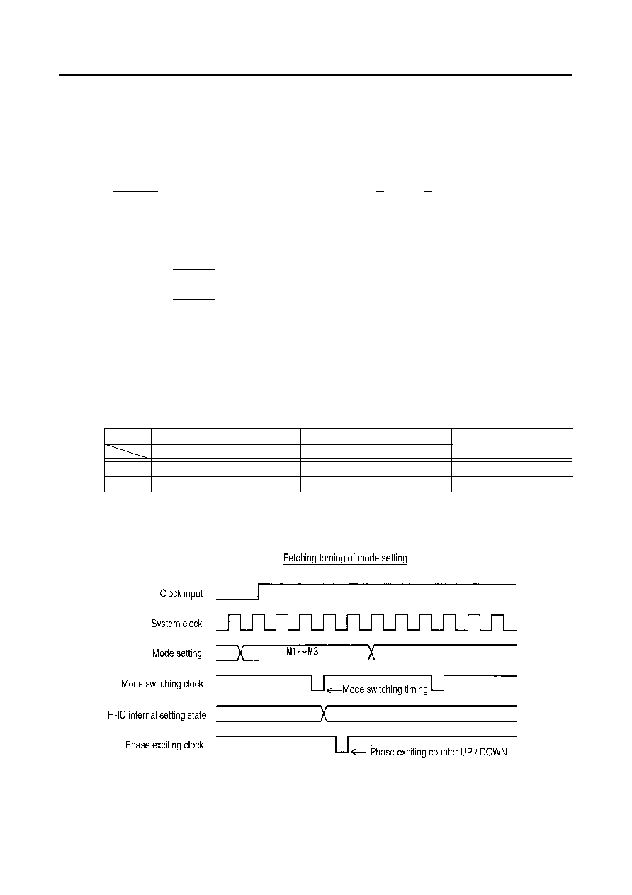
2-5. M1, M2, and M3 (Selection of exciting modes and clock input edge timing)
1. Pin format
s
CMOS Schmitt configuration containing the pull-up resistor
(20 k
typical value)
2. Functions
3. Valid timing of mode setting
s
The mode must not be changed within 5
µ
s from the leading edge and
trailing edge of the clock.
M2
0
0
1
1
Phase switching clock edge timing
0
1
0
1
1
2 phase exciting
1-2 phase exciting
W1-2 phase exciting
2W1-2 phase exciting
Only the leading edge
0
1-2 phase exciting
W1-2 phase exciting
2W1-2 phase exciting
4W1-2 phase exciting
Leading edge and trailing edge
M1
M3

STK672-040
No. 5227--7/11
2-6. M4 and M5 (Setting of rotation vector locus at micro-step)
For the current division ratio, see Section 4.3.
2-7. RESET (Reset of entire system)
1. Pin format
s
CMOS Schmitt configuration containing the pull-up resistor
(20 k
typical value)
2. Function
s
All circuit states are set to the initial values by setting the RESET signal to the
low state (pulse width of 10
µ
s or more). At this time, for all modes including
the exciting mode, the A and B phases are set to the origin.
2-8. Vref(Setting of the current value used as the reference of constant current detection)
1. Pin format
s
Analog input configuration
2. Function
s
By applying the voltage of 2.5 V or less of the control system power source
Vcc2, the constant current control can be performed over the exciting current of
the motor at the 100% of the rated current value.
s
The constant current can be controlled in proportional to the Vref voltage with
this value specified as a high limit.
3. Explanation of output pins
4. Functions and timing of output signals
4-1. A, A, B, and B (Output for phase exciting use of motor)
1. Function
s
In four phase two exciting mode, the interval of 3.75
µ
s (typical value)
is set when the output signals of the phases A and A, B and B change.
4-2. MO1, MO2, and MOI (Monitor of exciting state)
1. Pin format
s
CMOS standard configuration
2. Function
s
Outputs the state of the current phase exciting output.
For the MOI, 0 is output at the origin of each phase.
At other points, 1 is output.
M4
1
0
1
0
M5
1
0
0
1
Mode
Real circle
Pin No.
Name
Function
Pin format
19
MoI
Phase exciting origin monitor
CMOS standard configuration
20, 21
Mo1, Mo2
Phase exciting state monitor
CMOS standard configuration
Phase coordinate
A phase
B phase
A phase
B phase
Mo1
1
0
0
1
Mo2
0
1
0
1
STK672-040
No. 5227--8/11
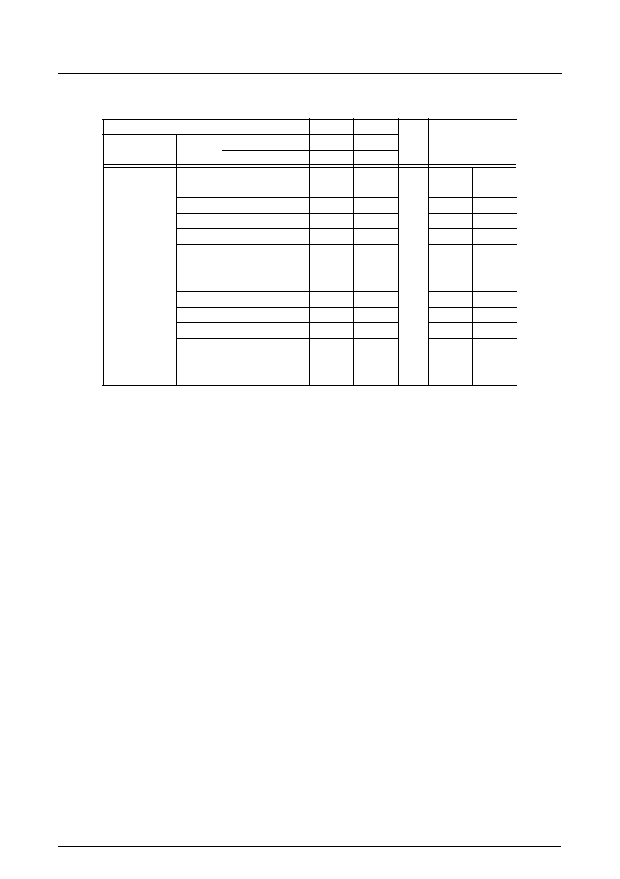
4-3. Current division ratio based on M3, M4, and M5 . . . . . . . . . . . . . . . . . . . Reference values
[Load conditions]
Vccl = 24V, Vcc2 = 5V, R / L = 3.5
/ 3.8mH
Mode
Real circle
Unit
Number of steps
Setting
M3 = 0
M3 = 1
M4 = 1
M4 = 0
M4 = 1
M4 = 0
M5 =1
M5 = 0
M5 =1
M5 = 0
Current division r
atio
4W1≠2
14
15
15
13
%
1 / 16
2W1-2
20
25
23
19
1 / 8
2 / 16
31
34
33
28
3 / 16
2W1-2
40
44
42
39
2 / 8
4 / 16
48
51
49
45
5 / 16
2W1-2
55
62
57
54
3 / 8
6 / 16
65
69
65
62
7 / 16
2W1-2
71
77
71
69
4 / 8
8 / 16
77
82
77
74
9 / 16
2W1-2
83
88
85
82
5 / 8
10 / 16
88
92
89
85
11 / 16
2W1-2
92
95
95
92
6 / 8
12 / 16
97
98
98
94
13 / 16
2W1-2
100
100
100
100
7 / 8
14 / 16
STK672-040
No. 5227--9/11
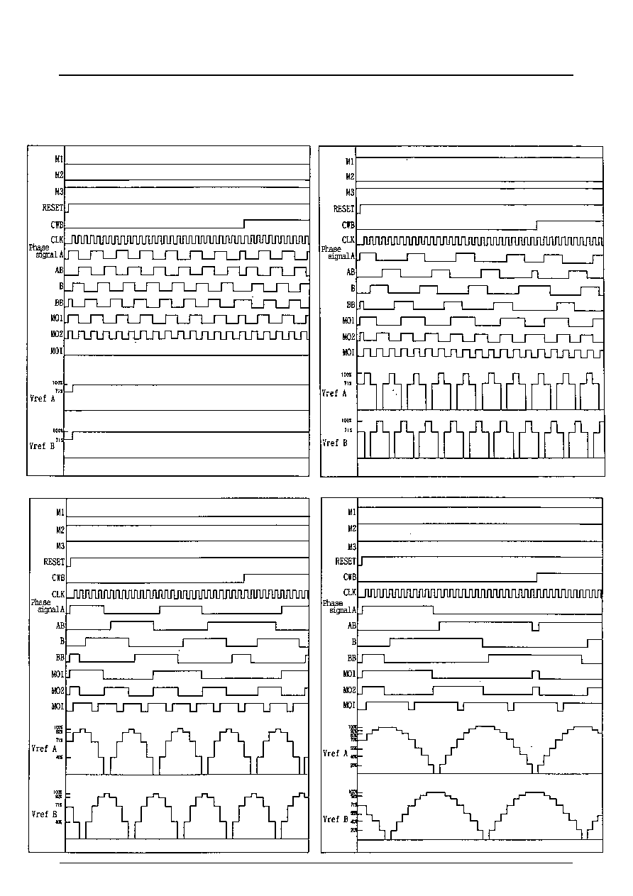
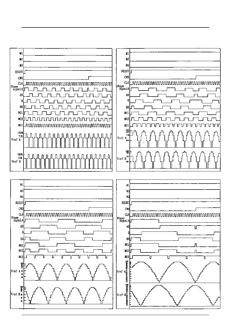
5. Phase exciting and timing chart
5-1. Leading edge operation of clock
∑ 2 phase exciting
∑ 1-2 phase exciting
∑ W1-2 phase exciting
∑ 2W-2 phase exciting
STK672-040
No. 5227--10/11
5-2. Leading edge and trailing edge operation of clock
∑ 2 phase exciting
∑ 1-2 phase exciting
∑ W1-2 phase exciting
∑ 2W-2 phase exciting

STK672-040
No. 5227--11/11
s
No products described or contained herein are intended for use in surgical implants, life-support systems, aerospace equipment, nuclear
power control systems, vehicles, disaster/crime-prevention equipment and the like, the failure of which may directly or indirectly cause injury,
death or property loss.
s
Anyone purchasing any products described or contained herein for an above-mentioned use shall:
Accept full responsibility and indemnify and defend SANYO ELECTRIC CO., LTD., its affiliates, subsidiaries and distributors and all their
officers and employees, jointly and severally, against any and all claims and litigation and all damages, cost and expenses associated
with such use:
Not impose any responsibility for any fault or negligence which may be cited in any such claim or litigation on SANYO ELECTRIC CO.,
LTD., its affiliates, subsidiaries and distributors or any of their officers and employees, jointly or severally.
s
Information (including circuit diagrams and circuit parameters) herein is for example only; it is not guaranteed for volume production. SANYO
believes information herein is accurate and reliable, but no guarantees are made or implied regarding its use or any infringements of
intellectual property rights or other rights of third parties.
This catalog provides information as of January, 1997. Specifications and information herein are subject to change without notice.